(China (Mainland))

Product Summary
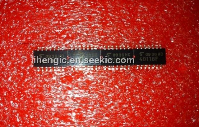
TC4011BF is 2-input positive logic NAND gate respectively. Since all the outputs of the TC4011BF are provided wirh the invertets as buffers, the input/output characteristics have been improved and the variation of propagation delat time due to the increase in load capacity is kept down to the minimum.
Parametrics
TC4011BF maximum ratings: (1) DC supply voltage VDD: Vss -0.5V to Vss +20V; (2) Input voltage VIN: Vss -0.5V to VDD +0.5V; (3) Output voltage VOUT: Vss -0.5V to VDD +0.5V; (4) DC input voltage IIN: ±10mA; (5) Power Disspation PD: 300 (DIP) /180 (SOIC) mW; (6) Operating temperature range Topr: -40 to 85°C; (7) Storage temperature range Tstg: -65 to 150°C.
Diagrams
| Image | Part No | Mfg | Description |  |
Pricing (USD) |
Quantity | ||||||
|---|---|---|---|---|---|---|---|---|---|---|---|---|
 |
 TC4011BFN |
Other |
|
Data Sheet |
Negotiable |
|
||||||
") |
TC4011BFN(F,N,M) |
|
IC GATE NAND QUAD 2INP 14-SOL |
Data Sheet |
Negotiable |
|
||||||
|
TC4011BFN(N,M) |
Toshiba |
IC GATE NAND QUAD 2INP 14-SOL |
Data Sheet |
|
|
||||||
|
TC4011BFT |
Other |
|
Data Sheet |
Negotiable |
|
||||||