(China (Mainland))

Product Summary
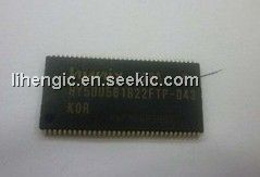
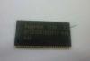
The HY5DU561622FTP-D43-C is a 268,435,456-bit CMOS Double Data Rate(DDR) Synchronous DRAM, ideally suited for the main memory applications which requires large memory density and high bandwidth. The HY5DU561622FTP-D43-CDDR SDRAM offers fully synchronous operations referenced to both rising and falling edges of the clock. The data paths are internally pipelined and 2-bit prefetched to achieve very high bandwidth. All input and output voltage level of the is compatible with SSTL_2.
Parametrics
HY5DU561622FTP-D43-C absolute maximum ratings: (1) Operating Temperature (Ambient) TA: 0 to 70°C; (2) Storage Temperature Tstg: -55 to 150°C; (3) Voltage on VDD relative to VSS, VDD: -1.0 to 3.6V; (4) Voltage on VDDQ relative to VSS, VDDQ: -1.0 to 3.6V; (5) Voltage on inputs relative to VSS VINPUT: -1.0 to 3.6V; (6) Voltage on I/O pins relative to VSS, VIO: -0.5V to 3.6V; (7) Output Short Circuit Current IOS: 50mA; (8) Soldering Temperature TSOLDER: 260°C.
Features
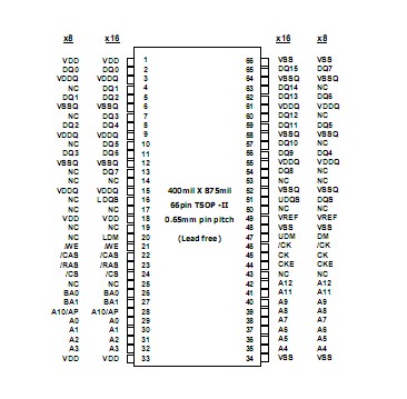
HY5DU561622FTP-D43-C features: (1) VDD, VDDQ = 2.5V +/- 0.2V for DDR200, 266, 333 VDD, VDDQ = 2.6V +0.1V / -0.2V for DDR400, 500; (2) All inputs and outputs are compatible with SSTL_2 interface; (3) Fully differential clock inputs (CK) operation; (4) Double data rate interface; (5) Source synchronous - data transaction aligned to bidirectional data strobe (DQS) ; (6) Data outputs on DQS edges when read (edged DQ) Data inputs on DQS centers when write (centered DQ) ; (7) DM mask write data-in at the both rising and falling edges of the data strobe; (8) All addresses and control inputs except data, data strobes and data masks latched on the rising edges of the clock; (9) Programmable CAS latency 2/2.5 (DDR200, 266,333) and 3 (DDR400, 500) supported; (10) Programmable burst length 2/4/8 with both sequential and interleave mode; (11) Auto refresh and self refresh supported; (12) JEDEC standard 400mil 66pin TSOP-II with 0.65mm pin pitch.
Diagrams