(China (Mainland))

Product Summary
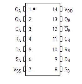
The MC14013B dual type D flip-flop is constructed with MOS P-channel and N-channel enhancement mode devices in a sing monolithic structure. The MC14013B has independent Data, (D) , Direct Set, (S) , Direct Reset, (R) , and Clock (C) inputs and complementary outputs (Q and Q) . The The MC14013B may be used as shift register elements or as type T flip¤Cflops for counter and toggle applications.
Parametrics
MC14013BCP absolute maximum ratings: (1) DC Supply Voltage Range VDD: -0.5V to +18V; (2) Input or Output Voltage Range (DC or Transient) Vin, Vout: -0.5V to VDD to +0.5V; (3) Input or Output Current (DC or Transient) per Pin Iin, Iout: ±10mA; (4) Power Dissipation, per Package PD: 500mW; (5) Ambient Temperature Range TA: -55 to 125°C; (6) Storage Temperature Range: -65 to 150°C; (7) Lead Temperature (8-Second Soldering) TL: 260°C.
Features
MC14013B features: (1) Static Operation; (2) Diode Protection on All Inputs; (3) Supply Voltage Range = 3.0Vdc to 18Vdc; (4) Logic Edge-Clocked Flip-Flop Design, Logic state is retained indefinitely with clock level either high or low; information is transferred to the output only on the positive-going edge of the clock pulse; (4) Capable of Driving Two Low-power TTL Loads or One Low-power Schottky TTL Load Over the Rated Temperature Range; (5) Pin-for-Pin Replacement for CD401.
Diagrams
| Image | Part No | Mfg | Description |  |
Pricing (USD) |
Quantity | ||||||||||||
|---|---|---|---|---|---|---|---|---|---|---|---|---|---|---|---|---|---|---|
 |
 MC14013BCP |
ON Semiconductor |
Flip Flops 3-18V CMOS Dual |
Data Sheet |
Negotiable |
|
||||||||||||
|
MC14013BCPG |
ON Semiconductor |
Flip Flops 3-18V CMOS Dual D-Type |
Data Sheet |
|
|
||||||||||||