(China (Mainland))


Product Summary
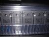
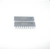
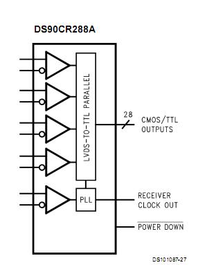
The DS90CR288AMTDX is a 3.3V rising edge data strobe LVDS 28-bit channel link. The DS90CR288AMTDX receiver converts the four LVDS data streams back into 28 bits of CMOS/TTL data. This chipset of the DS90CR288AMTDX is an ideal means to solve EMI and cable size problems associated with wide, high speed TTL interfaces.
Parametrics
DS90CR288AMTDX absolute maximum ratings: (1) SupplyVoltage (Vcc) : -0.3V to +4V; (2) CMOS/TTL Input Voltage: -0.5V to (Vcc +0.3V) ; (3) CMOS/TTL Output Voltage: -0.3V to (Vcc +0.3V) ;(4) LVDS Receiver Input Voltage: -0.3V to (Vcc +0.3V) ; (5) LVDS Driver Output Voltage: -0.3V to (Vcc +0.3V) ; (6) LVDS Output Short Circuit Duration: Continuous; (7) Junction Temperature: 150°C; (8) Storage Temperature: -65°C to +150°C; (9) Lead Temperature (Soldering, 4sec.) : +260°C; (10) Maximum Package Power Dissipation@+25°C, MTD56 (TSSOP) Package: 1.63W; (11) Package Derating: 12.4mW/°C above +25°C; (12) ESD Rating (HBM, 1.5kΩ, 100pF) >7kV, (EIAJ, 0Ω, 200pF) >700V, Latch Up Tolerance@±300mA.
Features
DS90CR288AMTDX features: (1) 20 to 85MHZ shift clock support; (2) 50% duty cycle on receiver output clock; (3) Best-in-Class Set&Hold Times on TxINPUTs; (4) Low power consumption; (5) ±1Vcommon mode range (around +1.2V) ; (6) Up to 2.38 Gbps throughput; (7) Upto 297.5 Megabytes/sec bandwidth; (8) Compatible with TIA/EIA-644LVDS standard; (9) Low profile5 6-lead TSSOP package; (10) 345mV (typ) swing LVDS devices forlow EMI.
Diagrams
| Image | Part No | Mfg | Description |  |
Pricing (USD) |
Quantity | ||||||||
|---|---|---|---|---|---|---|---|---|---|---|---|---|---|---|
 |
 DS90CR288AMTDX |
National Semiconductor (TI) |
LVDS Interface IC |
Data Sheet |
|
|
||||||||
 |
DS90CR288AMTDX/NOPB |
National Semiconductor (TI) |
LVDS Interface IC |
Data Sheet |
|
|
||||||||